SECURITIES AND EXCHANGE COMMISSION
Washington, D.C. 20549
FORM 6-K
REPORT OF A FOREIGN ISSUER
PURSUANT TO RULE 13A-16 OR 15D-16
OF THE SECURITIES EXCHANGE ACT OF 1934
For February 29, 2016
ASML Holding
N.V.
De Run 6501
5504 DR
Veldhoven
The Netherlands
(Address of principal executive offices)
Indicate by check mark whether
the registrant files or will file annual reports under cover of Form 20-F or Form 40-F.
Form 20-F x Form 40-F ¨
Indicate by check mark whether the registrant by furnishing the information contained in this Form is also thereby furnishing the information to the
Commission pursuant to Rule 12g3-2(b) under the Securities Exchange Act of 1934.
Yes ¨ No
x
If ‘‘Yes’’ is marked, indicate below the file number assigned to the
registrant in connection with Rule 12g3-2(b):
Exhibits
SIGNATURES
Pursuant to the requirements of the Securities Exchange Act of 1934, the registrant has duly caused this report to be signed on its behalf by
the undersigned, thereunto duly authorized.
|
|
|
|
|
|
|
|
|
|
|
ASML HOLDING N.V. (Registrant) |
|
|
|
|
| Date: February 29, 2016 |
|
|
|
By: |
|
/s/ Peter T.F.M. Wennink |
|
|
|
|
|
|
Peter T.F.M. Wennink |
|
|
|
|
|
|
Chief Executive Officer |
Exhibit 99.1
ASML Partners with Nippon Control System to Streamline Process Flow from Design to Mask Production
San Jose, California, 22 February 2016 – ASML Holding NV (ASML) today announced a partnership with Nippon Control System Corporation (NCS) to integrate
their products from optical proximity correction (OPC) to mask data preparation (MDP) on a common platform, delivering improvements in mask tape-out productivity and patterning performance in wafer fabrication. Semiconductor manufacturers will now
be able to deploy ASML’s computational lithography products and NCS’ MDP products into a seamless process flow for a faster and more accurate design to mask (D2M) solution.
The collaboration addresses the challenges customers are facing in mask tape-out and wafer patterning driven by growing mask complexity with shrinking process
nodes in both multiple patterning and EUV applications. Specific integration examples and benefits include:
| |
• |
|
A complete MDP flow to identify and improve mask accuracy required for pattern fidelity, critical dimension uniformity (CDU) and overlay performance; |
| |
• |
|
A seamless processing and handling of large volumes of data between OPC and MDP operations to reduce cycle time and optimize productivity, while maximizing utilization of available computing resources.
|
“By connecting ASML’s OPC and NCS’ MDP in an integrated tape-out flow, we have efficiently utilized computing clusters and
greatly reduced our design to mask cycle time,” said Laurent Tuo, Fellow and Technical Director at TSMC. “Such connectivity also enables mask process enhancements based on OPC output to deliver better imaging performance and more robust
process window.”
An integrated OPC and MDP solution is of greater importance for EUV lithography. “Mask proximity effects are stronger with
electron back scattering from the multi-layer mask stack composed of heavy metal elements,” said Nobuyasu Horiuchi, President of NCS. “An integrated EUV MDP solution flow will help accurately model and correctly handle mask making and
wafer imaging processes that impact CDU in EUV lithography.”
“Together with NCS, we are enabling complete solutions from design to mask and
driving wafer patterning performance to support our customers’ roadmaps at leading-edge nodes,” said Christophe Fouquet, Executive Vice President of Applications at ASML. “This partnership will further extend the scanner imaging and
overlay capabilities, by incorporating MDP in the holistic lithography solutions that consist of computational lithography, wafer lithography, metrology and process control.”
About Nippon Control System Corporation (NCS)
Nippon Control System Corporation (NCS) is a mask data preparation (MDP) software provider and has been providing MDP systems and fracturing tools to the
semiconductor industry since 1990. NCS offers NDE Mask Manufacturable Suite (NDE-MS) which includes all applications required by mask manufacturers after OPC and before mask writing. The applications are
NDE-Fracture, MRC, Select, Pattern-Match, SCRD, PEC, MPC, and View, supporting rule-based and model-based mask process correction (MPC), for both DUV and EUV mask
applications. For more information: http://www.nippon-control-system.co.jp
About ASML
ASML is one of the world’s leading manufacturers of chip-making equipment. Our vision is to enable affordable microelectronics that improve the quality of
life. To achieve this, our mission is to invent, develop, manufacture and service advanced technology for high-tech lithography, metrology and software solutions for the semiconductor industry. ASML’s guiding principle is continuing
Moore’s Law towards ever smaller, cheaper, more powerful and energy-efficient semiconductors. This results in increasingly powerful and capable electronics that enable the world to progress within a
multitude of fields, including healthcare, technology, communications, energy, mobility, and entertainment. We are a multinational company with over 70 locations in 16 countries, headquartered in Veldhoven, the Netherlands. We employ more than
14,000 people on payroll and flexible contracts (expressed in full time equivalents). ASML is traded on Euronext Amsterdam and NASDAQ under the symbol ASML. More information about ASML, our products and technology, and career opportunities is
available on: www.asml.com
Forward Looking Statements
This document contains statements relating to certain projections and business trends that are forward-looking, including statements with respect to
ASML’s partnership with NSC and the expected benefits from the partnership, including the expected performance and productivity improvements in semiconductor fabrication. You can generally identify these statements by the use of words like
“may”, “will”, “could”, “should”, “project”, “believe”, “anticipate”, “expect”, “plan”, “estimate”, “forecast”, “potential”,
“intend”, “continue” and variations of these words or comparable words. These statements are not historical facts, but rather are based on current expectations, estimates, assumptions and projections about the business and our
future financial results and readers should not place undue reliance on them. Forward-looking statements do not guarantee future performance and involve risks and uncertainties. These risks and uncertainties
include, without limitation, the risk that the expected benefits with respect to ASML’s partnership with NSC may not be realized and other risks indicated in the risk factors included in ASML’s Annual Report on Form 20-F and other filings with the US Securities and Exchange Commission. These forward-looking statements are made only as of the date of this document. We do not undertake to update or revise the forward-looking statements, whether as a result of new information, future events or otherwise.
2
Contacts
ASML
Niclas Mika
Corporate Communications
Contact Communications
+31 6 201 528 63
ASML
Brittney Wolff
Communication US
brittney.wolff.zatezalo@asml.com
+1 858 385 6502
ASML
Craig DeYoung
VP Investor Relations Worldwide
craig.deyoung@asml.com
+1.480.696.2762
ASML
Marcel Kemp
Director Investor Relations - Europe
marcel.kemp@asml.com
+31.40.268.6494
3
Exhibit 99.2
Forward Looking Statements
ASML
Public
This document contains statements relating to certain projections and business trends that are forward-looking, including statements with respect to productivity of our tools and
systems performance, EUV system performance, expected industry trends, and EUV targets (including availability, productivity and shipments) and roadmaps. You can generally identify these statements by the use of words like “may”,
“will”, “could”, “should”, “project”, “believe”, “anticipate”, “expect”, “plan”, “estimate”, “forecast”, “potential”, “intend”,
“continue” and variations of these words or comparable words. These statements are not historical facts, but rather are based on current expectations, estimates, assumptions and projections about the business and our future financial
results and readers should not place undue reliance on them. Forward-looking statements do not guarantee future performance and involve risks and uncertainties. These risks and uncertainties include, without limitation, the impact of manufacturing
efficiencies and capacity constraints, performance of our systems, the continuing success of technology advances and the related pace of new product development and customer acceptance of new products, the number and timing of EUV systems expected
to be shipped and recognized in revenue, delays in EUV systems production and development, our ability to enforce patents and protect intellectual property rights, the risk of intellectual property litigation, availability of raw materials and
critical manufacturing equipment and other risks indicated in the risk factors included in ASML’s Annual Report on Form 20-F and other filings with the US Securities and Exchange Commission. These forward-looking statements are made only as of
the date of this document. We do not undertake to update or revise the forward-looking statements, whether as a result of new information, future events or otherwise.
ASML
NXE 3300
Public
ASML
EUV lithography performance for manufacturing: status and outlook
Alberto Pirati
ASML Netherlands B.V., De Run 6501, 5504 DR Veldhoven, The Netherlands
SPIE 2016
ASML
Public
Slide 3
23 Feb 2016
Special appreciation to:
Matthew Colburn of IBM
Dan Corliss of IBM
Danilo de Simone of IMEC
Tony Yen of TSMC
Britt Turkot of Intel corporation
Chang Moon Lim of SK Hynix
Seong Sue Kim of Samsung Electronics
Andrew Grenville of Inpria
Martin Lowisch of Zeiss
ASML:
Rudy Peeters
Daniel Smith
Roderik van Es
Eric Verhoeven
Jo Finders
Arthur Minnaert
Marrit Hermens
Eelco van Setten
Lisa Mohanty
Jan-Willem van der Horst
Jan van Schoot
Jeannot Driedonkx
Sander Hofman
Niclas Mika
Bill Arnold
Derk Brouns
Joerg Mallmann
Daniel Brown
Christophe Smeets
Kars Troost
Rik Hoefnagels
Gijsbert Rispens
Raymond Maas
Hans Meiling
Judon Stoeldraijer
Herman Boom
Christian Wagner
Sjoerd Lok
Uwe Stamm
Michael Purvis
Alex Schafgans
Igor Fomenkov
Michael Lercel
David Brandt
Geert Fisser
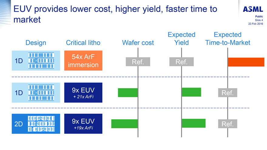
EUV provides lower cost, higher yield, faster time to market
ASML
Public
Slide 4
23 Feb 2016
1D
1D
2D
Design
Critical litho
54x ArF
immersion
9x EUV
+ 21x ArFi
9x EUV
+19x ArFi
Wafer cost
Ref.
Expected
Yield
Ref.
Expected
Time-to-Market
Ref.
Ref.
NXE extension roadmap to optimize capital efficiency
ASML
Public
Slide 5
23 Feb 2016
1st
Shipment
2013
20157
20175
2019
2021
Logic DRAM
R&D
D1H
D1M
D1L
3.x
<D1L
2~2.5
55 WpH
NXE:3300B
UVLS
SNEP 3350B
20% PFR illuminator
OFP 3350B 3400B
125 WpH
250W LPP
NXE:3350B
NXE:3400B
UVLS – Mk2
SMASH – MkX
Lens thermal
145 WpH
350W LPP
NXE: 3450C
500W source
Anamorphic lens
Stages, handlers
Products under study
185 WpH
Half pitch Focus
22 nm 16 nm 13 nm 13 nm <8 nm
DCO/MMO OPO
110 nm 3.0/5.0 nm 7.0 nm 70 nm
1.5/2.5 nm 3.5 nm
60 nm
1.4/<2.0 nm
2.5 nm
50 nm
1.2/<1.7 nm
2.0 nm
<40 nm
1.0/<1.4 nm
1.5 nm
See: 9776-55, Jan van Schoot “EUV high-NA scanner and mask optimization for sub-8nm resolution”
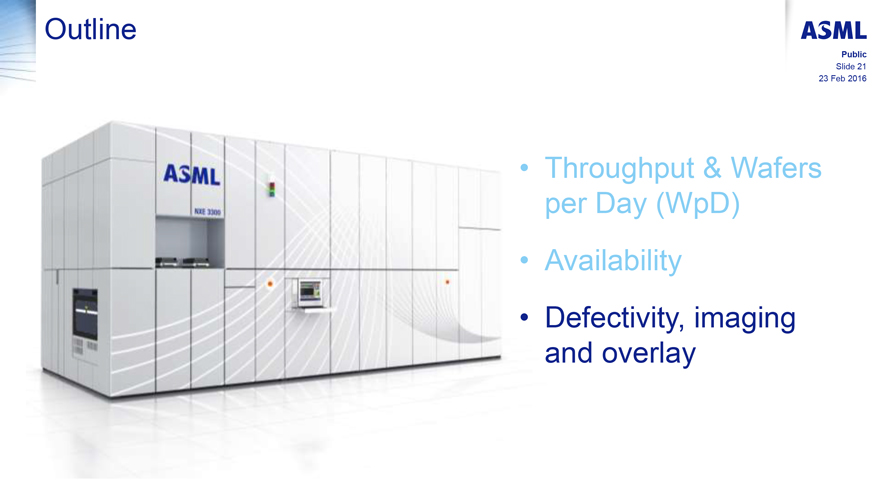
Outline
ASML NXE 3300
ASML
Public
Slide 6
23 Feb 2016
Throughput & Wafers per Day (WpD)
Availability
Defectivity, imaging and overlay
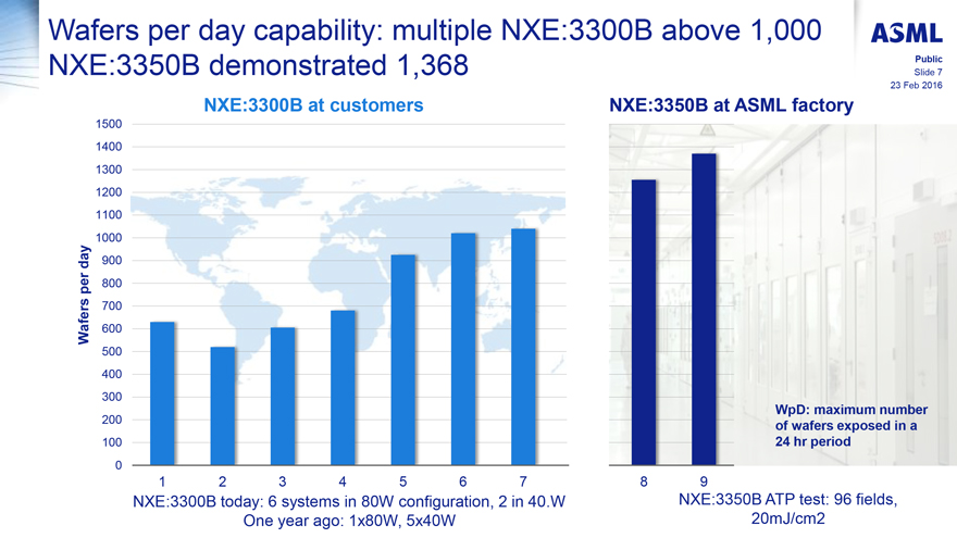
Wafers per day capability: multiple NXE:3300B above 1,000
NXE:3350B demonstrated 1,368
ASML
Public
Slide 7
23 Feb 2016
NXE:3300B at customers
NXE:3350B at ASML factory
1500
1400
1300
1200
1100
1000
day
900
per
800
700
Wafers
600
500
400
300
200
100
0
1
2
3
4
5
6
7
8
9
WpD: maximum number of wafers exposed in a
24 hr period
NXE:3300B today: 6 systems in 80W configuration, 2 in 40.W
One year ago: 1x80W, 5x40W
NXE:3350B ATP test: 96 fields,
20mJ/cm2
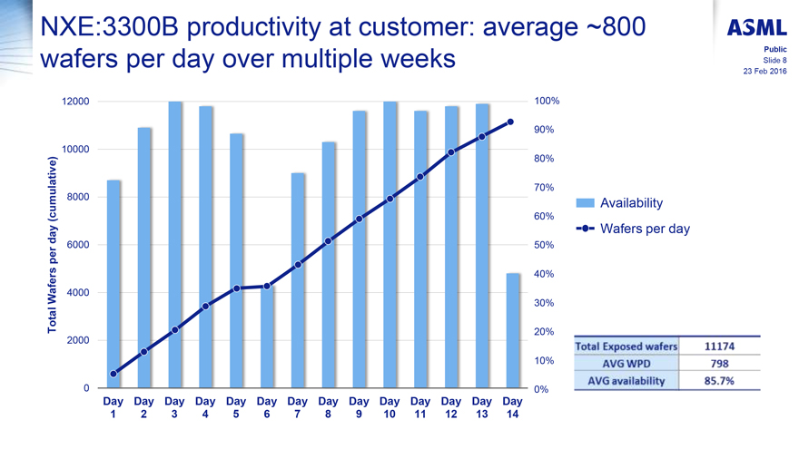
NXE:3300B productivity at customer: average ~800
wafers per day over multiple weeks
ASML
Public
Slide 8
23 Feb 2016
Total Wafers per day (cumulative)
12000
10000
8000
6000
4000
2000
0
100%
90%
80%
70%
60%
50%
40%
Availability
30%
Wafers per day
20%
10%
0%
Total Exposed Wafers
11174
AVG WPD
798
AVG availability
85.7%
Day Day Day Day Day Day Day Day Day Day Day Day Day Day
1 2 3 4 5 6 7 8 9 10 11 12 13 14
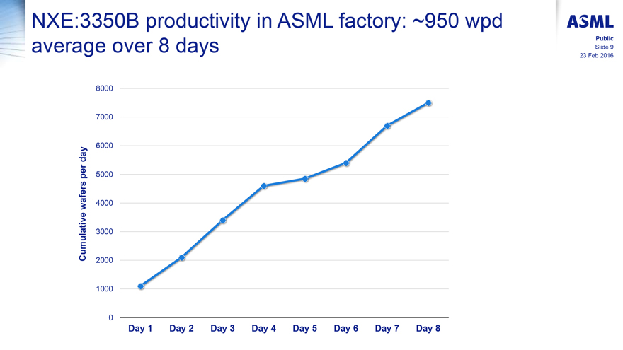
NXE:3350B productivity in ASML factory:
~950 wpd
average over 8 days
ASML
Public
Slide 9
23 Feb 2016
Cumulative wafers per day
8000
7000
6000
5000
4000
3000
2000
1000
0
Day 1
Day 2
Day 3
Day 4
Day 5
Day 6
Day 7
Day 8
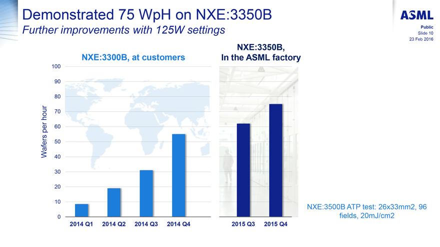
Demonstrated 75 WpH on NXE:3350B
Further improvements with 125W settings
ASML
Public
Slide 10
23 Feb 2016
Wafers per hour
NXE:3300B, at customers
NXE:3350B,
In the ASML factory
100
90
80
70
60
50
40
30
20
10
0
2014 Q1
2014 Q2
2014 Q3
2014 Q4
2015 Q3
2015 Q4
NXE:3500B ATP test: 26x33mm2, 96 fields, 20mJ/cm2
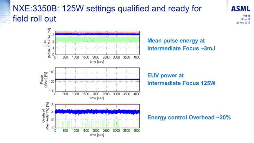
NXE:3350B: 125W settings qualified and ready for field roll out
ASML
Public
Slide 11
23 Feb 2016
Euv
(Mean+/-99.7%) [mJ]
0 1 2 3
0 500 1000 1500 2000 2500 3000 3500 4000
time [sec]
Mean pulse energy at Intermediate Focus ~3mJ
Power (Mean) [W]
140 120 100
0 500 1000 1500 2000 2500 3000 3500 4000
time [sec]
EUV power at Intermediate Focus 125W
Overhead
(Mean+/-99.7%) [%]
0 10 20 30
0 500 1000 1500 2000 2500 3000 3500 4000
time [sec]
Energy control Overhead
~20%
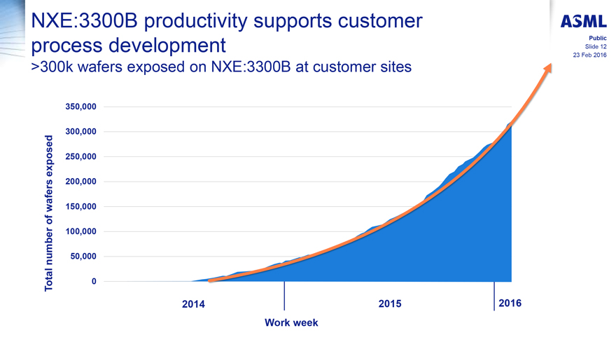
NXE:3300B productivity supports customer process development
>300k wafers exposed on NXE:3300B at customer sites
ASML
Public
Slide 12
23 Feb 2016
Total number of wafers exposed
350,000
300,000
250,000
200,000
150,000
100,000
50,000
0
2014
2015
2016
Work week
Acceleration in power scaling towards >200W builds further confidence in EUV productivity
ASML
Public
Slide 13
23 Feb 2016
240
220
3100 NOMO (delivered)
200
3100 MOPA (not shipped)
180
3100 MOPA+PP (not shipped)
See: 9776-21, Michael Purvis “Advances in predictive plasma
formation modelling”
160
3300 MOPA+PP (delivered)
See SPIE 2015, 9422-10, Alex Schafgans, “Performance optimization of MOPA pre-pulse LPP light source”
140
3400 MOPA+PP (development)
120
100
Power (Watts)
80
60
40
20
0
2008
2009
2010
2011
2012
2013
2014
2015
2016
2017
Outline
ASML
Public
Slide 14
23 Feb 2016
Throughput & Wafers per Day (WpD)
Availability
Defectivity, imaging and overlay
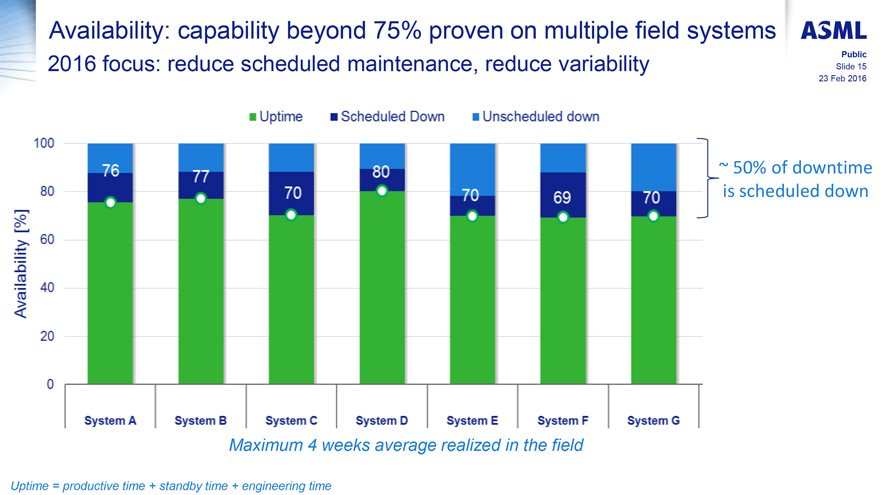
Availability: capability beyond 75% proven on multiple field systems
2016 focus: reduce scheduled maintenance, reduce variability
ASML
Public
Slide 15
23 Feb 2016
Uptime Scheduled Down Unscheduled down
Availability [%]
0 20 40 60 80 100
76 77 70 80 70 69 70
~50% of downtime is scheduled down
System A System B System C System D System E System F System G
Maximum 4 weeks average
realized in the field
Uptime = productive time + standby time + engineering time
Droplet Generator: Principle of Operation
ASML
Public
Slide 16
23 Feb 2016
Sn
Gas
Filter
Modulator
Nozzle
Tin is loaded in a vessel & heated above melting point
Pressure applied by an inert gas
Tin flows through a filter prior to the nozzle
Droplet
position,
m
10
5
0
-5
-10
0
5
10
15
20
25
30
Time, sec
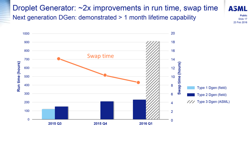
Droplet Generator: ~2x improvements in run time, swap time
Next generation DGen: demonstrated > 1 month lifetime capability
ASML
Public
Slide 17
23 Feb 2016
Run time (hours)
1000
900
800
700
600
500
400
300
200
100
0
Swap time
2015 Q3
2015 Q4
2016 Q1
20
18
16
14
12
10
8
6
4
2
0
Swap time (hours)
Type 1 Dgen (field)
Type 2 Dgen (field)
Type 3 Dgen (ASML)
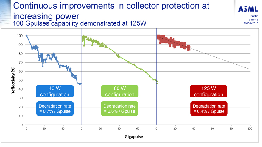
Continuous improvements in collector protection at increasing power
100 Gpulses capability demonstrated at 125W
ASML
Public
Slide 18
23 Feb 2016
Reflectivity [%]
100
90
80
70
60
50
40
30
20
10
0
0
20
40
0
20
40
60
0
20
40
60
80
100
40 W Configuration
Degradation rate = 0.7% / Gpulse
80 W Configuration
Degradation rate = 0.6% / Gpulse
125 W Configuration
Degradation rate = 0.4% / Gpulse
Gigapulse
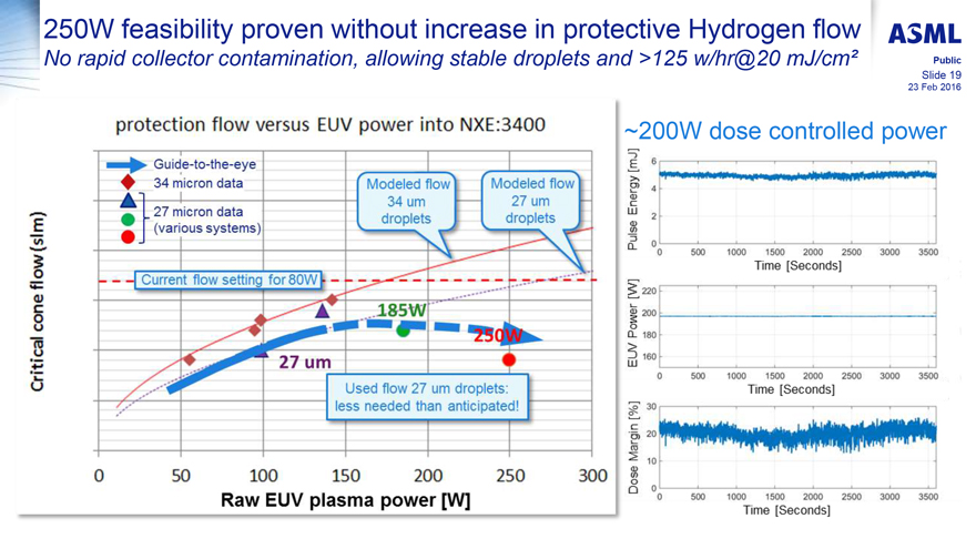
250W feasibility proven without increase in protective Hydrogen flow
No rapid collector contamination, allowing stable droplets and >125 w/hr@20 mJ/cm²
ASML
Public
Slide 19
23 Feb 2016
protection flow versus EUV power into NXE:3400
Critical cone flow (slm)
Guide-to-the-eye
34 micron data
27 micron data
(various systems)
Current flow setting for 80W
27 um 185 W 250 W
Used flow 27 um droplets: less needed than anticipated!
Modeled flow 34 um droplets
Modeled flow 27 um droplets
0
50
100
150
200
250
300
~200W dose controlled power
Pulse Energy [mJ]
6
4
2
0
0
500
1000
1500
2000
2500
3000
3500
Time [Seconds]
EUV Power [W]
220
200
180
160
0
500
1000
1500
2000
2500
3000
3500
Time [Seconds]
Dose Margin [%]
30
20
10
0
0
500
1000
1500
2000
2500
3000
3500
Time [Seconds]
Raw EUV plasma power [W]
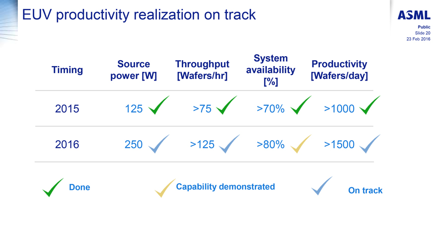
EUV productivity realization on track
ASML
Public
Slide 20
23 Feb 2016
Timing
Source power [W]
Throughput [Wafers/hr]
System availability [%]
Productivity [Wafers/day]
2015
125
>75
>70%
>1000
2016
250
>125
>80%
>1500
Done
Capability demonstrated
On track
Outline
ASML
Public
Slide 21
23 Feb 2016
Throughput & Wafers per Day (WpD)
Availability
Defectivity, imaging and overlay
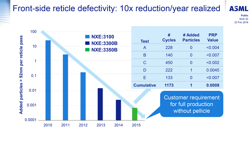
Front-side reticle defectivity: 10x reduction/year realized
ASML
Public
Slide 22
23 Feb 2016
Added particles > 92nm per reticle pass
100
10
1
0.1
0.01
0.001
0.0001
2010 2011 2012 2013 2014 2015
NXE:3100
NXE:3300B
NXE:3350B
Test
A
B
C
D
E
Cumulative
#
Cycles
228
140
450
222
133
1173
# Added
Particles
0
0
0
1
0
1
PRP
Value
<0.004
<0.007
<0.002
0.0045
<0.007
0.0008
Customer requirement for full production without pellicle
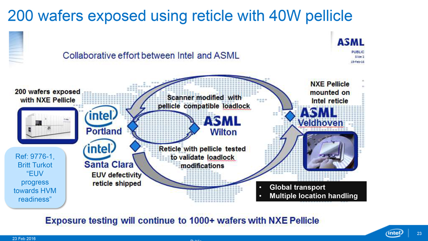
200 wafers exposed using reticle with 40W pellicle
ASML
Public
Slide 2
19 Feb 2016
Collaborative effort between Intel and ASML
200 wafers exposed with NXE Pellicle
Ref: 9776-1,
Britt Turkot
“EUV
progress towards HVM
readiness”
intel Portland
intel Santa Clara
EUV defectivity reticle shipped
Scanner modified with pellicle compatible loadlock
ASML
Wilton
Reticle with pellicle tested to validate loadlock modifications
NXE Pellicle mounted on Intel reticle
ASML
Veldhoven
Global transport
Multiple location handling
Exposure testing will continue to 1000+ wafers with NXE Pellicle
23 Feb 2016
intel
23
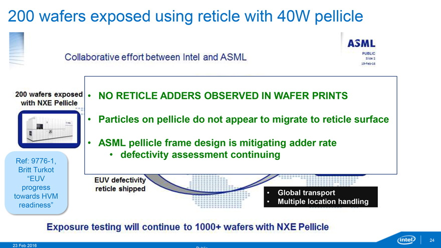
200 wafers exposed using reticle with 40W pellicle
ASML
Public
Slide 24
19 Feb 2016
Collaborative effort between Intel and ASML
200 wafers exposed with NXE Pellicle
Ref: 9776-1,
Britt Turkot
“EUV
progress towards HVM
readiness”
NO RETICLE ADDERS OBSERVED IN WAFER PRINTS
Particles on pellicle do not appear to migrate to reticle surface
ASML pellicle frame design
is mitigating adder rate
defectivity assessment continuing
EUV defectivity
reticle shipped
Global transport
Multiple location handling
Exposure testing will continue to 1000+ wafers with NXE Pellicle
23 Feb 2016
intel
24
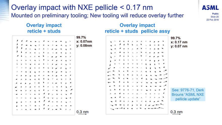
Overlay impact with NXE pellicle < 0.17 nm
Mounted on preliminary tooling; New tooling will reduce overlay further
ASML
Public
Slide 25
23 Feb 2016
Overlay impact reticle + studs
99.7%
x: 0.07nm
y: 0.08nm
0.3 nm
Overlay impact reticle + studs pellicle assy
99.7%
x: 0.17 nm
y: 0.07 nm
See: 9776-71, Derk
Brouns “ASML NXE pellicle update”
0.3nm
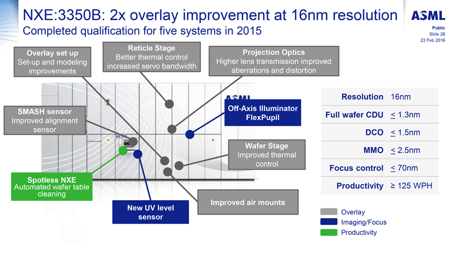
NXE:3350B: 2x overlay improvement at 16nm resolution
Completed qualification for five systems in 2015
ASML
Public
Slide 26
23 Feb 2016
Overlay set up
Set-up and modeling improvements
SMASH sensor
Improved alignment sensor
Spotless NXE
Automated wafer table cleaning
Reticle Stage
Better thermal control increased servo bandwidth
New UV level sensor
Projection Optics
Higher lens transmission improved aberrations and distortion
Off-Axis Illuminator FlexPupil
Wafer Stage
Improved thermal control
Improved air mounts
Resolution 16nm
Full wafer CDU £ 1.3nm
DCO £ 1.5nm
MMO £ 2.5nm
Focus control £ 70nm
Productivity ³ 125 WPH
Overlay
Imaging/Focus
Productivity
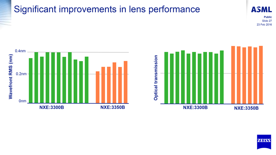
Significant improvements in lens performance
ASML
Public
Slide 27
23 Feb 2016
Wavefront RMS (nm)
0.4nm 0.2nm 0nm
NXE:3300B NXE:3350B
Optical transmission
NXE:3300B NXE:3350B
ZEISS
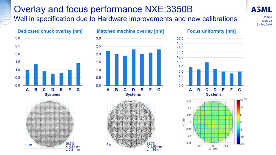
Overlay and focus performance NXE:3350B
Well in specification due to Hardware improvements and new calibrations
Dedicated chuck
overlay [nm]
3.0
2.5
2.0
1.5
1.0
0.5
0.0
ABCDEFG
Matched machine overlay [nm]
3.0
2.5
2.0
1.5
1.0
0.5
0.0
ABCDEFG
Focus uniformity [nm]
20.2
18.0
16.0
14.0
12.0
10.0
8.0
6.0
4.0
2.0
0.0
ABCDEFG
Systems
4 nm
99.7%
X:0.84 nm
Y: 0.81 nm
Systems
4 nm
99.7%
X: 1.59 nm
Y: 1.86 nm
System
Y (m)
0.15
01
0.05
0
-0.05
-0.1
-0.15
-0.1
0
0.1
15
nm
10
5
0
-5
-10
-15
X (m)
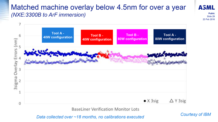
Matched machine overlay below 4.5nm for over a year
(NXE:3300B to ArF immersion)
ASML
Public
Slide 29
23 Feb 2016
3sigma Overlay Errors (nm)
76543210
Tool A - 40W configuration
Tool B - 40W configuration
Tool B - 80W configuration
Tool A - 80W configuration
X 3sig
Y 3sig
BaseLiner Verification Monitor Lots
Courtesy of IBM
Data collected over ~ 18 months, no calibrations executed
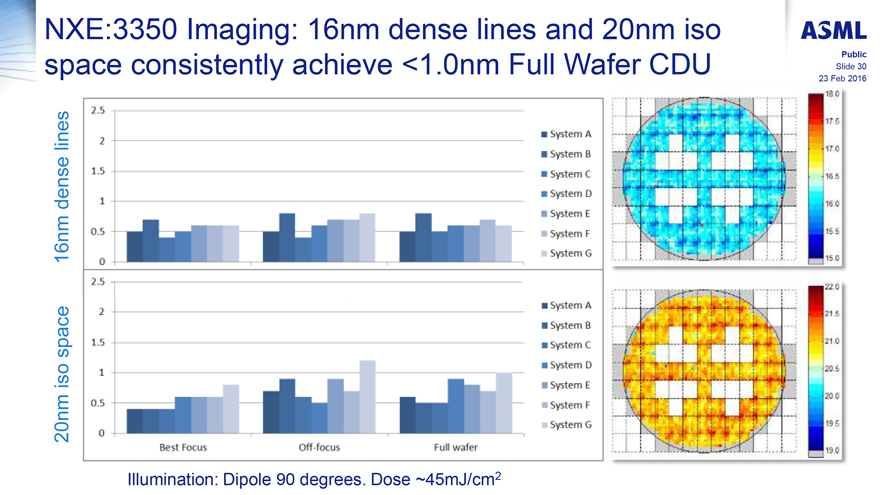
NXE:3350 Imaging: 16nm dense lines and 20nm iso space consistently achieve <1.0nm Full Wafer CDU
ASML
Public
Slide 30
23 Feb 2016
16 nm dense lines
2.5
2 System A
1.5 System B
1 System C
0.5 System D
System E
System F
0 System G
20 nm is so space
2.5 System A
2 System B
1.5 System C
1 System D
0.5 System E
System F
0 System G
Best Focus
Off-focus
Full wafer
18.0
17.5
17.0
16.5
16.0
15.5
15.0
22.0
21.5
21.0
21.5
20.5
20.0
19.5
19.0
Illumination: Dipole 90 degrees. Dose ~45mJ/cm2
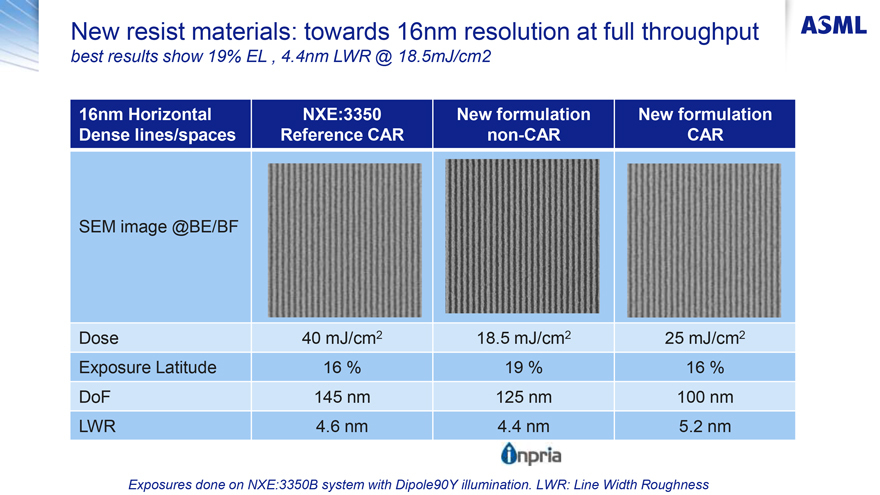
New resist materials: towards 16nm resolution at full throughput
best results show 19% EL, 4.4nm LWR @ 18.5mJ/cm2
ASML
|
| 16nm Horizontal Dense lines/spaces NXE:3350 Reference CAR New formulation non-CAR New formulation CAR |
| SEM image @BE/BF |
| Dose 40 mJ/cm2 18.5 mJ/cm2 25 mJ/cm2 |
| Exposure Latitude 16% 19% 16% |
| DoF 145 nm 125 nm 100 nm |
| LWR 4.6 nm 4.4 nm 5.2 nm |
inpria
Exposures done on NXE:3350B system with
Dipole90Y illumination. LWR: Line Width Roughness
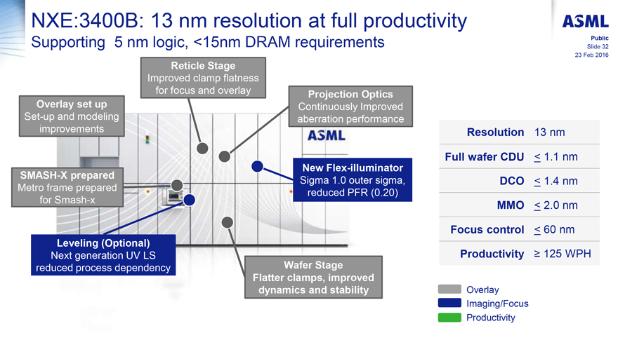
NXE:3400B: 13 nm resolution at full productivity
Supporting 5 nm logic, <15nm DRAM requirements
ASML
Public
Slide 32
23 Feb 2016
Reticle Stage
Improved clamp flatness for focus and overlay
Overlay set up
Set-up and modeling improvements
Projection Optics
Continuously Improved
aberration performance
SMASH-X prepared
Metro frame prepared for Smash-x
New Flex-illuminator
Sigma 1.0 outer sigma, reduced PFR (0.20)
Leveling (Optional)
Next generation UV LS reduced process dependency
Wafer Stage Flatter clamps, improved dynamics and stability
|
|
|
| Resolution |
|
13 nm |
| Full wafer CDU |
|
£ 1.1 nm |
| DCO |
|
£ 1.4 nm |
| MMO |
|
£ 2.0 nm |
| Focus control |
|
£ 60 nm |
| Productivity |
|
³ 125 WPH |
Overlay
Imaging/Focus Productivity
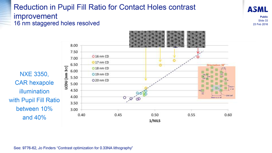
Reduction in Pupil Fill Ratio for Contact Holes contrast improvement
16 nm staggered holes resolved
ASML
Public
Slide 33
23 Feb 2016
NXE 3350,
CAR hexapole
illumination
with Pupil Fill Ratio
between 10%
and 40%
LCDU [nm 3]
8.00
7.50
7.00
6.50
6.00
5.50
5.00
4.50
4.00
3.50
3.00
16 nm CD
17 nm CD
18 nm CD
19 nm CD
20 nm CD
0.40
0.45
0.50
0.55
0.60
1/NILS
See: 9776-62, Jo Finders “Contrast optimization for 0.33NA lithography”
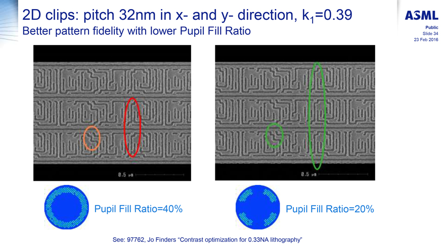
2D clips: pitch 32nm in x- and y- direction, k1=0.39
Better pattern fidelity with lower Pupil Fill Ratio
ASML
Public
Slide 34
23 Feb 2016
0.5
0.5
Pupil Fill Ratio=40%
Pupil Fill Ratio=20%
See: 97762, Jo Finders “Contrast optimization for 0.33NA
lithography”
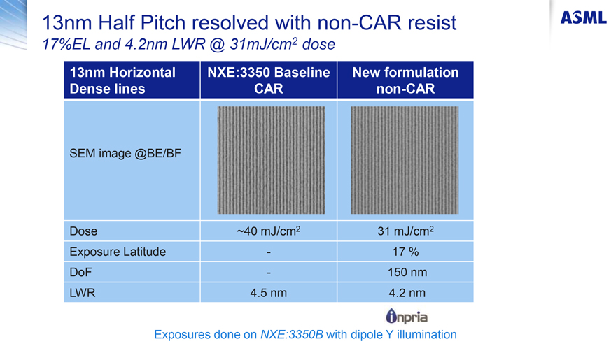
13nm Half Pitch resolved with non-CAR resist
17%EL and 4.2nm LWR @ 31mJ/cm2 dose
ASML
|
| 13nm Horizontal NXE:3350 Baseline New formulation |
| Dense lines CAR non-CAR |
| SEM image @BE/BF |
| Dose ~40 mJ/cm2 31 mJ/cm2 |
| Exposure Latitude - 17% |
| DoF - 150 nm |
| LWR 4.5 nm 4.2 nm |
Inpria
Exposures done on NXE:3350B with dipole Y
illumination
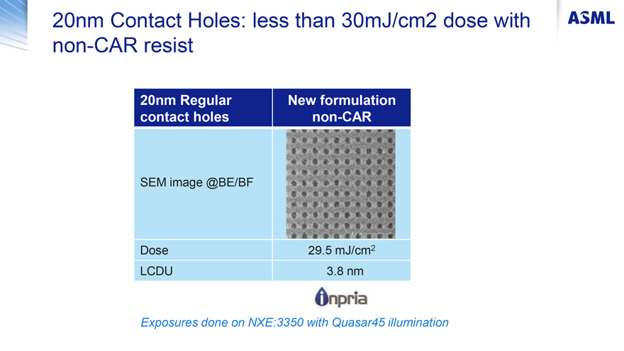
20nm Contact Holes: less than 30mJ/cm2 dose with non-CAR resist
ASML
|
| 20nm Regular New formulation |
| contact holes non-CAR |
| SEM image @BE/BF |
| Dose 29.5 mJ/cm2 |
| LCDU 3.8 nm |
Inpria
Exposures done on NXE:3350 with Quasar45
illumination
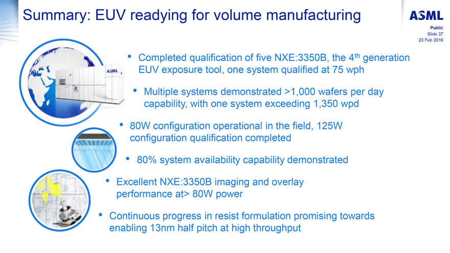
Summary: EUV readying for volume manufacturing
ASML
Public
Slide 37
23 Feb 2016
Completed qualification of five NXE:3350B, the 4th generation EUV exposure tool, one system qualified at 75 wph
Multiple systems demonstrated >1,000 wafers per day capability, with one system exceeding 1,350 wpd
80W configuration operational in the field, 125W configuration qualification completed
80%
system availability capability demonstrated
Excellent NXE:3350B imaging and overlay performance at> 80W power
Continuous progress in resist formulation promising towards enabling 13nm half pitch at high throughput
Exhibit 99.3
ASML share buy back program
Repurchase up to €
1.5 billion in the 2016 - 2017 timeframe
|
|
|
| Announced 20 January 2016 |
|

|
Repurchased of total program: 7.9%
|
|
|
|
|
|
|
|
|
|
|
|
|
| Date |
|
Repurchased shares |
|
|
Average price |
|
|
Repurchased value |
|
| 21 Jan - 22 Jan 2016 |
|
|
30,500 |
|
|
€ |
80.03 |
|
|
€ |
2,440,778 |
|
| 25 Jan - 29 Jan 2016 |
|
|
238,037 |
|
|
€ |
82.35 |
|
|
€ |
19,601,768 |
|
| 1 Feb - 5 Feb 2016 |
|
|
629,144 |
|
|
€ |
80.94 |
|
|
€ |
50,923,321 |
|
| 8 Feb - 12 Feb 2016 |
|
|
455,063 |
|
|
€ |
74.86 |
|
|
€ |
34,066,035 |
|
| 15 Feb - 19 Feb 2016 |
|
|
154,911 |
|
|
€ |
75.58 |
|
|
€ |
11,707,596 |
|
|
|
|
|
| Total |
|
|
1,507,655 |
|
|
€ |
78.76 |
|
|
€ |
118,739,497 |
|
ASML Holding NV (NASDAQ:ASML)
Historical Stock Chart
From Mar 2024 to Apr 2024

ASML Holding NV (NASDAQ:ASML)
Historical Stock Chart
From Apr 2023 to Apr 2024
